Introduction to Inverter Circuits
Digital equipment relies on Inverter circuits because they change DC inputs into AC outputs. People use these versatile systems in many different ways because they form the essential foundation for two basic to advanced equipment types, including simple inverter . Everyone who practices or studies electronics relies on inverter circuit diagram understanding to design, enhance or repair these systems.
Inverter technology grows rapidly because people depend on it more for renewable energy installations plus backup power and portable electronics. Inverters change DC power from batteries and solar panels into AC power, creating output waveforms that power stations and electronics need to work.
This complete document covers all parts of inverter circuit diagrams including essential basics and complex realizations. Our article gives important ideas about simple inverter circuits and how they work both to beginners and skilled engineers.
Fundamentals of Inverter Operation

Basic Principles of DC to AC Conversion
The basic function of an inverter involves its capacity to convert one-directional direct current into alternating current that can reverse direction and flips direction repeatedly. DC current used in power circuits must be interrupted through switching mechanisms to produce the oscillating pattern of AC power.
The main idea behind these inverters works when fast semiconductor switches control the movement of DC power through an inverter transformer. Switch operation at defined intervals allows inverters to produce AC power while specifying its amperage range, cycles per second and output pattern. The control circuit decides all key output qualities so it stands as the core part of an inverter system.
Types of Inverter Waveforms
Inverter output power varies based on how the device is built and what it is designed to do.
- Square Wave Inverters: create a basic repetitive rectangle waveform voltage output. You get the most basic control at a low price but the output distorts power to the point it works for only lights and crude motors.
- Modified Sine Wave Inverters: It produces an approximation of a sine wave through its stepped Modified Sine Wave function. Modified sine wave inverters deliver decent performance and save money while working well with everyday appliances except those that require high precision technology.
- Pure Sine Wave Inverters: Sine Wave Inverters produce a perfectly round electricity pattern that matches normal power connections. They can serve any electrical need including medical gear yet medical gear without generating distortions but their advanced configuration adds to their higher price.
- Grid-Tie Inverters: Grid-Tie Inverters allow renewable systems to support the power grid while sending extra power back to it.
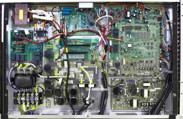
Key Components in Inverter Circuits
The common parts of typical inverter circuits consist of these parts:
- DC Power Source: Typically batteries, solar panels, or DC generators
- Oscillator Circuit: Generates the base frequency for the inverter operation
- Power transistors and other semiconductor elements such as MOSFETs IGBTs and thyristors are used for actual power switching operations
- These components link power switches to the control system inside the inverter.
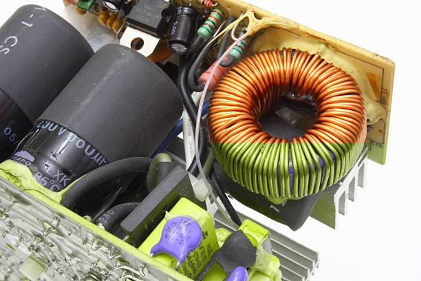
- Transformer: Provides isolation and voltage step-up/down functionality
- The filter circuits regulate the output signal to decrease harmonics.
- Michaelcontrollers and dedicated Integrated Circuits handle power switch patterns.
- The safety system protects the power components from overloads and abnormal situations such as short circuits.
Analyzing how the different parts work together through the circuit diagram provides the basis for successful inverter development or repair.
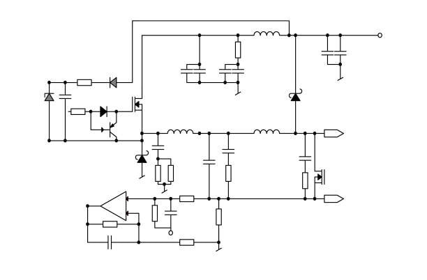
Basic Inverter Circuit Diagrams
Simple Transistor-Based Inverter
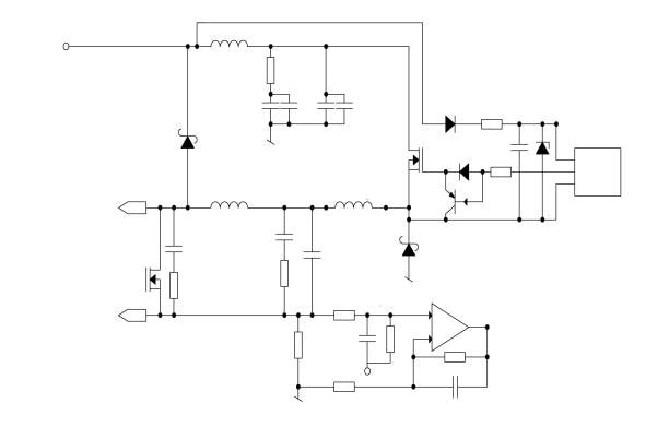
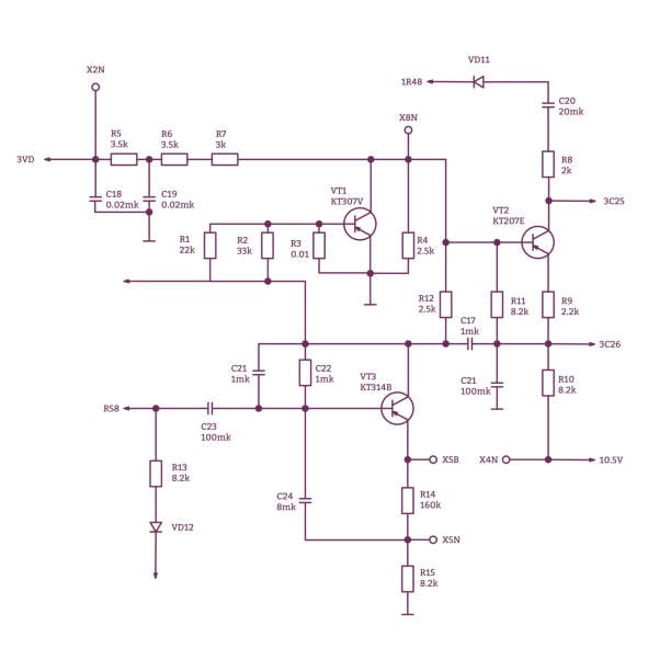
A basic inverter circuit system pairs two transistors as push-pull units to switch energy between a center-tapped transformer’s halves. The transistors transmit electrical energy one at a time sending current through different sections of the transformer primary circuit. The transformer core generates an AC voltage in the secondary winding due to its exposure to the alternating magnetic field produced by the primary part.
Basic oscillator circuits usually consist of 555 timers as well as multivibrator designs to power transistors in their operation. This first design shows the basic functions of inverters and provides a starting point for additional advanced circuits.
MOSFET-Based Inverter Circuits
MOSFET-based switching technology provides modern inverters better performance and supports applications like low battery management because of its superior switching capabilities and high efficiency. The basic MOSFET inverter utilizes these essential components, including mosfet transistors :
- A pair of N-channel MOSFETs for the switching operation
- The system requires gate drivers to control MOSFET functionality
- Input protection and filtering components
- Output transformer for voltage conversion
- Feedback mechanisms for output regulation
The circuit diagram of an MOSFET inverter shows only the parts that manage MOSFET gate drive power and timing to avoid short circuits.
H-Bridge Inverter Configuration
H-bridge stands as a versatile inverter design with four switching elements laid out in an H pattern. These four components allow electrical power to move both forward and reverse through the device to change battery voltage from DC to AC power.
The H-bridge circuit uses four switches connected to both the DC source and the load targets. By controlling the switching sequence:
- Switches 1 and 4 ON, 2 and 3 OFF: Current flows one direction through the load
- Switches 2 and 3 ON, 1 and 4 OFF: Current flows in the opposite direction
- The system needs to turn off all switches at once during dead time to stop electric flow.
The basic setup of four switches builds the base for power converter development in multiple systems such as variable drives, solar power systems, and power backup devices.
Single-Phase Inverter Diagrams
Half-Bridge Inverter Design
The half-bridge inverter makes the most of economics by linking only two switching devices to a divided DC power source. The circuit divides the DC bus into two parts through capacitors to generate a low cost center point gezhen as the neutral reference.
These switches follow an opposite pattern with each other since one device must be active while the other stays inactive. The switching sequence links the electrical load either to positive or negative parts of the DC power supply and produces an alternating voltage. Despite being less complex than H-bridges the half-bridge circuit has specific usage restrictions.
- The system can effective use only the lower half of its voltage input
- Separating the DC supply needs additional capacitors for this process.
- The capacitor equipment needs to manage large power supply variations
Half-bridge inverters work in UPS systems and audio amplifiers along with other low-performance applications, but pure sine wave inverters are preferred for high-quality output.
Full-Bridge Inverter Layout
The full-bridge inverter made of four switches makes conversion more efficient while offering better flexibility in power control. The H-bridge topology allows the full amount of DC bus voltage to be exploited for generating double the output voltage possibilities.
The full-bridge inverter circuit allows several switching methods to appear in its setup.
- Two opposing switches work as a pair to make the output voltage go from one end to the other of DC bus voltage
- Unipolar Switching techniques generate multiple supply zero states which reduce harmonic power usage and increase overall device efficiency.
The full-bridge design achieves better results but needs two times the number of switches and more advanced control algorithms than a half-bridge setup.
Push-Pull Inverter Configuration
Push-pull inverters transfer power effectively between a DC source and single-phase transformer circuits by using two switches with a center-tapped transformer. In the layout diagram both switches switch between DC source and opposite transformer primary ends to produce alternating core flux.
This configuration offers several advantages:
- The transformer core works better when put to use properly
- Simple control requirements
- Good voltage utilization
Despite these benefits the push-pull design faces the issue of transformer core saturation when switches operate incorrectly. The circuit outline includes supplementary parts to avoid core saturation problems such as current sensing units and timing adjustment circuits.
Three-Phase Inverter Diagrams
Three-Phase Bridge Inverter
People use three-phase inverters for industrial motor drives and utility-level renewable power systems including solar power applications and lead acid battery setups. The simple three-phase bridge inverter uses six switching devices arranged as one half-bridge unit for each output phase.
The drawing shows how each phase connects its pair of switches directly between the positive and negative DC bus. Each leg in the bridge contains two switches that synchronize their actions to produce equal three-phase AC power.
In current three-phase inverter layouts you will find these components.
- The design requires six electronic power-control devices (IGBTs or MOSFETs).
- Electrical components control the functioning of each power switch
- DC bus capacitors for energy storage and ripple reduction
- Current sensors for feedback and protection
- Output filters to reduce harmonics
The controls of three-phase inverters demand advanced processing because they need space vector modulation and similar advanced methods to reach high efficiency levels.
Six-Step VSI Circuit
The fundamental three-phase inverter control method is the six-step voltage source inverter structure. The inverter circuit structure repeats the basic three-phase bridge design but requires specific six-step switching actions.
During each one-third cycle the output phases connect to positive or negative DC buses sequentially exhausting all 6 possible states. Because of its easy setup this method creates excessive harmonics in the output signal that need filtration to work with delicate equipment.
The basic circuit contains built-in blocking networks to guard against stress that occurs during six-step control switching operations.
PWM Three-Phase Inverter Design
The advanced Pulse Width Modulation method represents the top-level control technology for three-phase inverters. The basic three-phase inverter circuit stays the same but PWM technologies use complex control systems including astable multivibrator to swiftly control power device switches and generate sinusoidal output voltages.
The PWM inverter circuit design features main parts that require specific attention.
- Control signal generation and isolation
- Heat dissipation from the switching devices
- The system blocks electrical and radio noise generated during power switching.
- The output filter system transforms the uneven chopping from the input.
Most updated three-phase inverters with PWM technology use microcontrollers or DSP processors for creating advanced output patterns through sinusoidal PWM, space vector modulation, and selective harmonic removal.
Multilevel Inverter Circuits
Diode-Clamped Multilevel Inverter
Multilevel inverters produce better sine wave outputs by using multiple voltage levels in power conversion. With diode-clamped multilevel inverters (also known as neutral-point clamped or NPC inverters) additional diodes are added to control output voltage levels.
A three-level diode-clamped inverter circuit diagram contains four main switching devices plus two clamping diodes and two DC bus capacitors that create a neutral point.
- Four main switching devices
- Two clamping diodes
- Two DC bus capacitors form a common point for neutralization
This design connects each output phase to positive DC bus, neutral point, or negative DC bus creating a three-level waveform with lower harmonics than normal two-level inverters.
Adding more output levels requires more capacitors and diodes which makes the circuit control system more challenging as the number of levels increases.
Flying Capacitor Multilevel Inverter
A flying capacitor multilevel inverter produces intermediate voltage levels through the use of capacitors instead of diodes. The circuit design reveals how capacitors maintain different voltage levels across them to produce multiple output voltages.
A single phase flying capacitor inverter system employs three voltage levels which need specific circuits.
- Four main switching devices
- One floating capacitor per phase
- Advanced systems monitor voltage between capacitor power sources
Before use the floating capacitors require correct preset voltages and the system must efficiently switch to keep them at these levels. The additional control complexity of flying capacitor inverters makes them better suited for handling substantial power requirements compared to diode-clamped devices.
Cascaded H-Bridge Multilevel Inverter
A cascaded H-bridge inverter supports multiple output phases by joining brand-new H-bridge cells in series. Every cell unit adds its unique voltage level to form the full output signal pattern.
A cascaded H-bridge inverter needs half of the DC sources minus one
source and H-bridge modules for each phase in its N-level design. This system arrangement brings many benefits to the design.
- Inherent fault tolerance through redundancy
- Scalability to very high voltage applications
- Lots of independent renewable power sources can operate each module
By using the cascaded H-bridge design many solar arrays or battery banks directly power one H-bridge unit in renewable high-power applications.
Control Circuit Diagrams for Inverters
Analog Control Circuits
While most modern inverters use digital control systems analog circuits maintain their value for specific applications because they are simple to design, cost-effective and reliable. An ordinary analog control circuit design for inverters contains these parts.
- The oscillator system makes base frequency electricity.
- Sensor conditioners depend on operational amplifiers and voltage-comparators to perform their role.
- Reference voltage generators
- Feedback loops for regulation
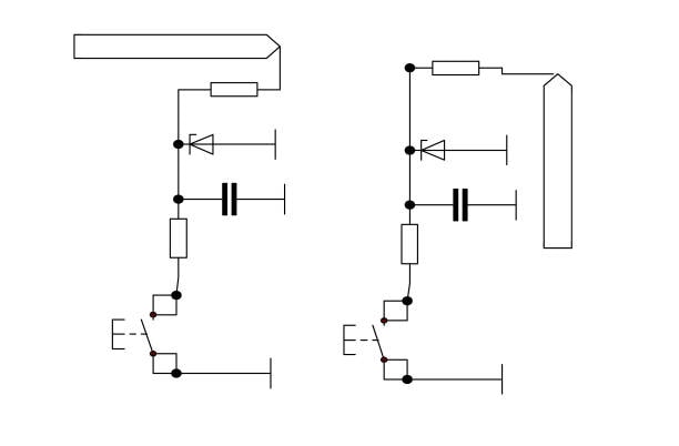
- Dead-time generators to prevent shoot-through
- Protection circuits for overcurrent and overvoltage conditions
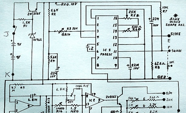
Analog control chips specially created for inverters operate in inverter systems through products like the SG3524, TL494, or IR2110 series. These integrated circuits include necessary features for power inverters to create simpler and more dependable systems.
Digital PWM Controllers
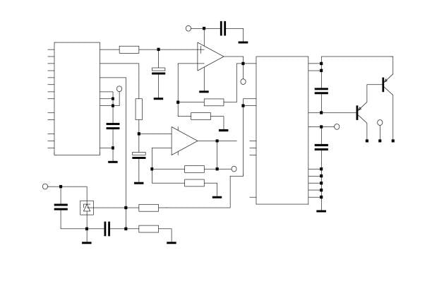
Digital control systems now lead all inverters worldwide because they guarantee exceptional performance customization. A power inverter digital control system shows how digital signals connect with power stage components.
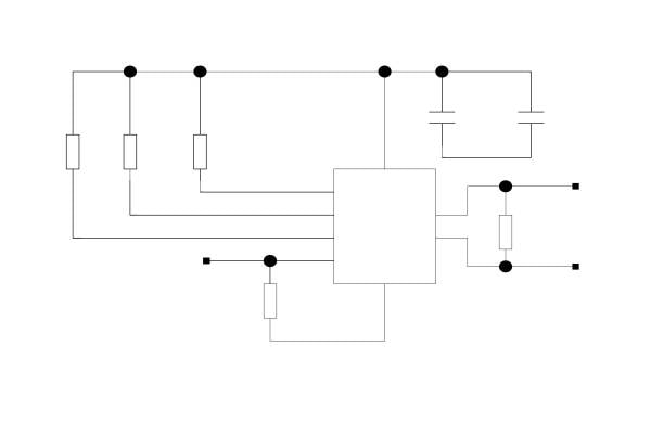
A normal digital control portion includes these components.
- Microcontroller or DSP as the central processing unit
- Special digital converters help detect electrical voltage and current levels
- Gate driver interface circuits
- Communication interfaces (RS-485, CAN, Ethernet)
- User interface components
- Memory for parameter storage
Modern computer systems use various complex algorithms that digital controllers run better than analog systems for tasks like self-adjusting dead time control and fault identification while reducing electrical harmonics. The circuit diagram needs to add safety measures for signal isolation, noise protection, voltage drop and stable operation.
Microcontroller-Based Inverter Control
Modern inverters mostly use microcontroller-based control systems because these systems provide excellent performance combined with flexible capabilities and reasonable costs. A standard microcontroller-based inverter controller circuit layout has these particular components:
- A microcontroller with PWM circuit support functions (lengthy control systems from AVR and PIC to ARM and specific DSP types)
- An electrical barrier separates the controller and power parts of the system.
- Sensor conditioning circuits
- Protection and monitoring components
- Communication interfaces
The microcontroller runs programmed commands to adjust system readings and control PWM signals for proper output performance. The electrical design must include proper grounding techniques to prevent digital noise interference from reaching the power components and vice versa.
Special-Purpose Inverter Diagrams
Grid-Tie Inverter Circuits
The purpose of grid-tie inverters is to connect to the electric grid and supply power back to it while working in synchronization. The main circuit components of grid-tie inverters differ from standalone units since grid connection needs special electronics.
- Phase-locked loop (PLL) circuits for grid synchronization
- Anti-islanding protection
- Power quality monitoring
- Grid connection relays or contactors
- DC injection prevention circuits
- Compliance monitoring for grid codes
The graphic layout shows these inverters operate back and forth since they need to shift DC power into AC energy while tracking grid measurements and managing faulty behavior. These safety systems need to operate with public power networks since they handle direct power connections.
UPS Inverter Systems
UPS inverter systems need to supply reliable electricity during power failure periods and complete the transition between grid power sources very quickly. The UPS inverter system circuit diagram displays this requirement by containing
- Battery charging circuits
- Automatic transfer switches
- Status monitoring and indication
- Battery health monitoring
- Bypass systems for maintenance
- Communication interfaces for remote monitoring
The basic parts of UPS inverter circuit diagrams remain consistent but their complexity grows based on the offline, line-interactive or online doubles conversion topologies to quickly react to power changes and regulate the battery charge.
Motor Drive Inverter Circuits
AC motors receive their speed and torque adjustments through the use of inverters in variable frequency drives. Their design layouts demonstrate how motors need particular control solutions.
- The breaking chopper device converts motor energy into electrical power
- Motor parameter sensing
- Specialized PWM patterns for motor control
- Speed and position feedback interfaces
- The system includes special security mechanisms designed for motor power systems
Field-oriented control and direct torque control algorithms need fast processing and exact timing to operate in motor drive inverters. Our design needs to handle tough industrial conditions, incorporating heat sinks, and fulfill the described performance requirements in the main circuit diagram.
Protection Circuits in Inverter Diagrams
Overcurrent Protection Designs
Protection against excessive current represents a fundamental requirement for any inverter system. An electrical network uses multiple ways to protect against overcurrent issues.
- Current sensing resistors or transformers
- Hall effect sensors
- Fast-acting fuses
- Electronic current limiting
- Circuit breakers
- Crowbar circuits for catastrophic failure modes
The circuit diagram explains how protection elements interact with the control system to adjust the output as an overcurrent event happens while also shutting everything down when needed.
Overvoltage Protection Mechanisms
Voltage shocks will harm the inverter unit and other linked items. The diagram for inverters displays various protection against high voltages arranged in multiple levels.
- Metal oxide varistors (MOVs)
- Transient voltage suppressors (TVS diodes)
- Zener diode clamps
- RC or LC snubber networks
- Software-based voltage monitoring and shutdown
Different protection elements throughout the circuit diagram guard both the inverter inputs and outputs plus manage any sensitive control areas.
Thermal Management in Inverter Circuits
Heat stands as one of the major causes of power electronics failure. Inverter circuit diagrams use these features to control heat buildup during operations.
- Temperature sensing devices (thermistors, thermocouples)
- Fan control circuits
- Thermal shutdown pathways
- Power derating algorithms
- Heatsink connections and thermal interfaces
The symbols used to represent physical cooling elements in the circuit diagram show their complete electrical control and monitoring systems necessary for thermal protection.
Advanced Inverter Circuit Techniques
Resonant Inverter Topologies
Resonant inverters use LC tanks to switch devices softly and decrease both power dissipation and electrical noise creation. The resonant inverter circuit highlights the key tank components and their connections to the switching devices, which may produce a square wave output .
Common resonant inverter topologies include:
- Series resonant inverters
- Parallel resonant inverters
- Series-parallel (LLC) resonant inverters
- Zero voltage switching (ZVS) configurations
- Zero current switching (ZCS) arrangements
A correct circuit diagram needs to show the exact values of resonant components since they decide how the inverter operates and switches.
Soft-Switching Inverter Designs
Switching losses diminish when soft-switching systems prevent voltage spikes and current flows across the switching devices during their transition periods. Soft-switching inverters need special components added to their circuit diagrams to enable efficient operation while minimizing square wave distortions .
- Auxiliary switches and resonant components
- Special timing units guide the switching elements at exact times
- Snubber networks
- Saturable inductors or magnetic components
- Energy recovery circuits
The supplementary components raise circuit complexity but let us achieve better efficiency and suppress electromagnetic interference at high switching rates, through the use of a secondary transformer .
High-Frequency Inverter Circuits
Inverters with high switching frequencies run at frequencies of 10 to 100 kHz which makes magnetic components small and allows faster control. Their illustrations show particular circuit setups specifically chosen for this application.
- High-speed switching devices (typically MOSFETs)
- Low-inductance layout considerations
- The circuitrys of gates drive power need special support for faster operation
- EMI filtering components
- These magnetic parts are made for work at high radio wave frequencies
The circuit design for high-frequency inverters requires specific attention to parasitic elements because they affect performance at higher frequencies through stray inductance and capacitance effects in all electrical conductors.
Practical Inverter Design Considerations
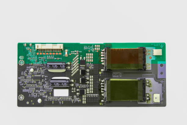
PCB Layout Guidelines for Inverter Circuits
PCB design decisions are essential for inverter success although they do not appear on the circuit diagram. When creating circuit diagrams extra layers note how to design the printed circuit board in key areas.
- Power and ground plane design
- Component placement for thermal management
- Critical signal path routing
- EMI/RFI considerations
- High-current trace requirements
- Sealed shielding separates electronics for power delivery from electronic control units
Current inverter systems combine their circuit diagrams with design maps to teach engineers how to make theory real in hardware.
Thermal Design Considerations
Controlling heat becomes fundamental when building inverters. The thermal design aspects of circuits take the following measures in our diagrams.
- Thermal sensor placement and connections
- Fan control circuitry
- Temperature-dependent protection logic
- Thermal relief in power connections
- Component derating specifications
These features provide protection against temperature-related issues so the inverter works without thermal runaway problems while preserving its components for longer use.
EMC and Noise Reduction Techniques
EMC considerations take top position in inverter circuit designs to handle both electrical noise emitted through cables and radio transmitters.
- Common mode and differential mode filter components
- Shielding connections
- Ferrite components for noise suppression
- Ground arrangement and star points
- Filter capacitor placement and selection
EMC planning needs to align with design needs which makes the circuit diagrams complicated with added filters and suppressors.
Reading and Interpreting Inverter Circuit Diagrams
Common Symbols in Inverter Schematics
Different industries and regions use specific symbols when designing inverter circuits for their standard parts. Common symbols include:
- Semiconductor switches (diodes, transistors, MOSFETs, IGBTs)
- Passive components (resistors, capacitors, inductors)
- Transformers and magnetic components
- Protection devices (fuses, circuit breakers)
- Measurement and sensing elements
- Control components and integrated circuits
The connections between basic symbols in an inverter circuit determine how to properly read and understand its design.
Block Diagram vs. Detailed Circuit Representation
Inverter documents contain layout diagrams and full circuit blueprints alongside each other.
- The block diagram displays how different main subsystems work together.
- The complete circuit diagrams show exact placement and specs of each circuit part
- Circular diagrams connect high and low level views in a step-by-step progression
The several representations help people understand and solve inverter problems while making design changes. These representations together show all elements of how the inverter system operates.
Troubleshooting Using Circuit Diagrams
The circuit diagram helps electrical workers find and fix inverter issues. You can fix inverter issues better by studying circuit diagrams through these actions
- Our process includes finding areas to check if components perform as expected.
- Understanding signal flow and expected waveforms
- Learning to spot protection circuits plus their activation signals
- We identify separate blocks in the designs to test them efficiently.
- Our analysis detects possible component failures from how the circuit parts are connected.
These professional inverter circuit designs provide detailed information about how a system should work under normal conditions as part of their troubleshooting materials.
Future Trends in Inverter Circuit Design
Wide-Bandgap Semiconductor Integration
The use of silicon carbide and gallium nitride wide-bandgap semiconductors improves how inverters are designed. The next-generation inverter designs contain these new features require ac power.
- Simplified gate drive requirements for some devices
- Reduced or eliminated snubber circuits
- The higher switching speed helps reduce component size in the circuit.
- These units require specific safety solutions that depend on their using components’ special properties.
- The new cooling systems need development based on unique thermal characteristics
The growth of modern inverter technology requires updates to its circuit diagrams that enhance how semiconductor devices handle heat and adjustments.
Integrated Inverter Modules
Today’s inverter development features power modules that pack various components together. New circuits display both traditional and integrated module thermal control technologies power transformer.
- The circuit diagram connects all integrated modules within the system.
- Simplified external circuitry
- Digital communication with embedded controllers ferrite core transformer
- Standardized protection and monitoring features
- Reduced component count for peripheral functions input voltage
The integrated power module trend makes circuit diagrams simpler and boosts reliability because of less connections and standardized manufacturing processes for internal parts output frequency.
Smart Inverter Communication Protocols
New inverters come with built-in network features and advanced methods to transmit information. The plans for intelligent inverters show these components inside power output.
- The circuits process communication data through RS-485, CAN, Ethernet, WiFi, and Bluetooth interfaces.
- Protocol translator ICs
- Isolation for communication links
- Security features for data protection
- Remote monitoring and control capabilities
The communication features let inverters connect to energy networks to help run the grid system and deliver precise monitoring data for improvement, including output current insights output ac voltage .
Conclusion
The representations of Inverter circuits require knowledge across power electronics science control theory and actual engineering practices. Despite starting simple transistor structures transistors have evolved through sophisticated multilevel digital controls into fundamental electrical power structures.
To understand inverter circuit diagrams you need to combine knowledge of semiconductor physics with magnet design principles and both electronic control systems and how they avoid electromagnetic interference. The complexity of current inverter designs shows how much today’s technology meets upgradeable specifications.
The growth of renewable energy technologies and electric vehicles will keep inverter systems as core builders of electrical engineering developments. The electrical designs progress through developing diagrams with upgraded components for enhanced output performance, including features for low battery management .
Knowing how inverters work from their electrical plans creates the basics needed to use these common power conversion tools in engineering.